


Circuit board manufacturing requires a lot of expenses, especially for mass production. Read this article from FS Technology to reduce your manufacturing costs. In this article, we will detail common design mistakes in PCB manufacturing and assembly.

For wholesale PCBA projects, FS Technology believes that design defects are the most fatal error in the entire PCBA manufacturing process due to poor design before production. For finished product sellers, it is very unfavorable to redesign or choose other PCBA manufacturers, which will directly increase R&D and time costs. Prototyping is, therefore, necessary to test the entire design before proceeding to wholesale PCBA. FS Technology believes that the best way to test is to apply Design for Manufacturing (DFM) and Design for Assembly (DFA) rules when designing the board layout.
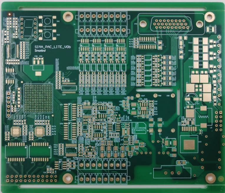
Design Phase of High Volume PCB Manufacturing
DFM is a design guide for PCB designers to identify printed circuit board boards, which points out errors that may occur during the manufacturing process. In order to make the manufactured PCBA suitable for electronic products, we need to spend a lot of time reading and correcting errors. For a turnkey PCB manufacturer like FS Technologies, we have our own unique DFM checklist to follow. Note: Here we are talking about the production of bare printed circuit boards.
The following are common problems in wholesale PCBA manufacturing:
PCBA Design files that are not good
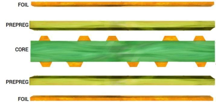
Gerber and ODB++ files contain important information that you need to focus on, such as layer images, board outlines, IPC netlists, master diagrams, and layer order.
The production stage will be at risk due to confusion of manufacturing specifications.
The PCBA material selection was wrong
The requirements for the board do not match the requirements for the project. It is important to use boards that are capable of handling high- frequencies, such as ceramic PCBs.
When you talk with suppliers about material requirements, pick the right PCB material at the first stage.

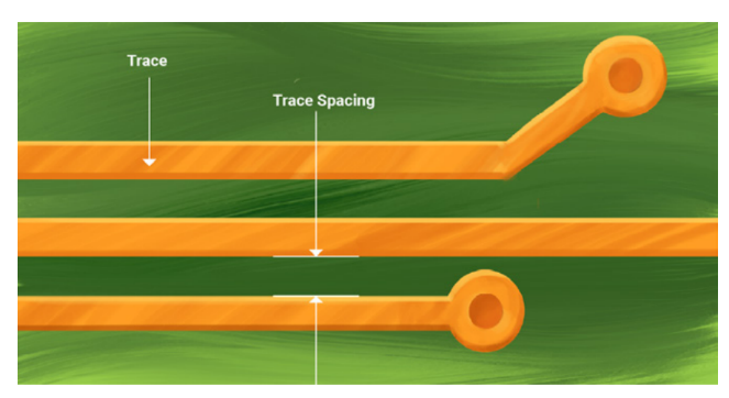
Wrong PCBA Trace Width
Circuit boards have copper traces, which are necessary to connect all components in the circuit. Affected signal transmission, short circuit board, or heat dissipation problems are caused by trace defects.
The conductor’s current carrying capacity is determined by the trace width. Their relationship is positive and the stronger the trace, the more current-carrying capacity they have.
The board gets hotter when it cannot carry the higher current.
To get the trace width of the side of the circuit board to be greater than 4 mil, you have to rationally adjust the conductor width.
You can use online tools to boost trace width, current capacity, and temperature rise if you don’t know.
Wrong PCBA Trace Spacing
The spacing of the traces should be kept reasonable in order to avoid a circuit layout that is too small.
There’s too dense a trace distance to cause flashover and crosstalk.
You should provide clearance between conductors, following standard guidelines.
The conductor spacing and voltage calculator are the same as the trace width calculator and can be used to calculate the optimal spacing between conductors.

PBCA Drilling Error
Through holes and alignment are some of the purposes for which manufacturers drill holes in printed circuit boards. The process of drilling is irreversible and any drilling you have to do will ruin your design. The board size, pitch, aspect ratio, number of holes on the board and machine type are other factors that can be considered. Common mistakes that affect drilling are insufficient hole and drill-to- copper distance. Learn about your manufacturer’s drilling techniques and specifications once you are in contact with them.
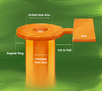

Specifications for drilling vias
Annular ring placement
PCBA Solder Mask Errors
The mask protects the PCBA from becoming contaminated and insulates it from connecting to the rest of the world. The manufacturer shows where the components are placed for the soldering process. There is no clearance between the via mask openings and the adjacent component openings, which may cause solder bridges to form. Poor solder joints can result from this.


CAM snapshot of a solder bridge
An inadequate solder mask can lead to the formation of a solder opening and it will expose the copper to attack from the elements.
PCBA Copper and solder mask slivers
Copper shards formed during the printing stage are termed copper slivers. These pieces of metal will be lifted off and fall into the bath. The photoresistChunks can deposit anywhere on the board, making them a potential leading to shorts. The areas where photoresist is removed may affect the board’s function.
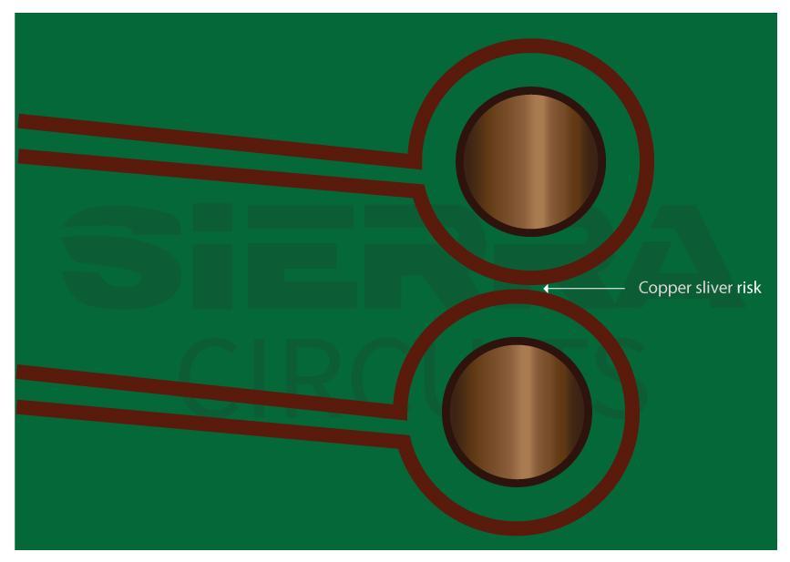

Copper sliver risk
A chance that the lightly bonded dams are no more than 4 mils is certain when they are less than a year old.
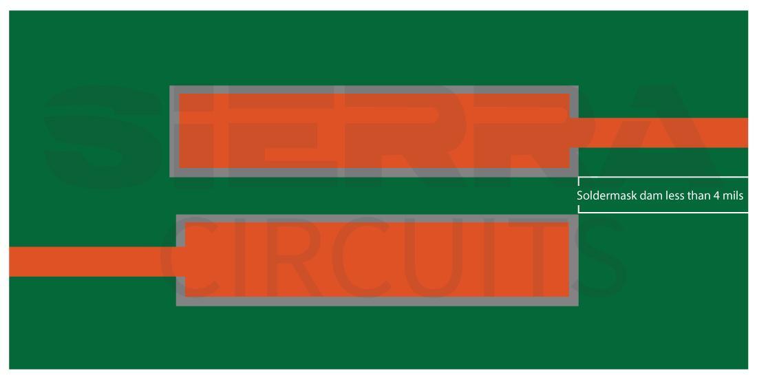

Solder mask sliver risk
PCBA Starved thermals
The process of soldering can damage a board. To avoid this you have to provide the appropriate thermal relief padding. FS Technologies found that the heat-dissipating copper spokes on the thermal pads can help with heat transfer. When there are no thermals on an airplane, we call this phenomenon a starvation thermal. The boards we use can overheat from these hungry heat.

Disconnected thermals
PCB Design-for-Assembly
The reality of the sculptures and productions we design is addressed through the assembly design process. Check the availability and placement of the component here. The feasibility of production and other parts of assembly are examined. Understanding DFA will help you simplify the PCBA layout and reduce the chance of design failure. There is a difference between the assembly in DFA and the one in this article: the process of soldering all of the components onto the PCBA.
PCBA Data inefficiency
DFM and other similar design processes require that you verify all the basic data sheets. The key parameters include package dimensions, data, sini data, part numbers, etc. You avoid future mistakes if you do this.
Choosing the wrong components
We are influenced by part selection when assembling. Through-hole components require complex manufacturing processes compared to surface mount technology. It is best to use them when you need them. There are lots of standard elements that are available from multiple vendors. Since you can only source parts from certain suppliers, they are often not suitable for large production and can add to the cost.
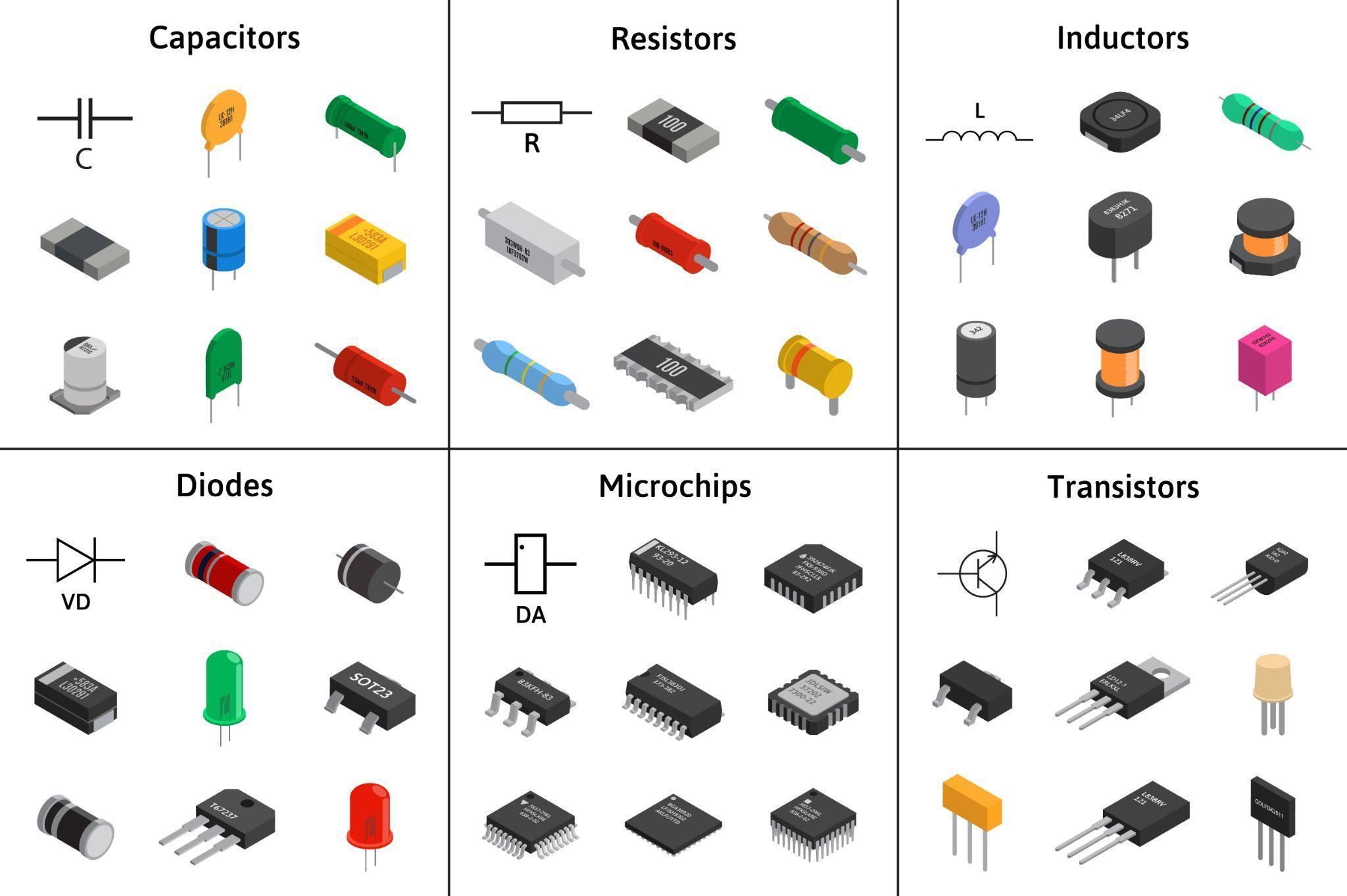

Different types of components are available
PCBA Component availability
You must always confirm the availability of parts before you start making a bill of materials. The cost estimation with the help of the BOM checker.
PCBA Incorrect footprint
We give the components needed to assemble the board in the BOM file. The circuit will be more difficult to complete if the component shape in the BOM does not match the data in the package.
Insufficient component spacing
There is insufficient spacing during component installation. Adequate spacing between parts to facilitate manual soldering and have extra space for sensitive components such as QFPO, POP or BGA. We sometimes need to place elements close together to achieve a low form factor. It is best to follow spacing guidelines.
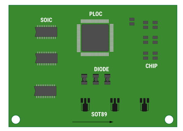

Standard component placement
PCBA Inadequate component to edge spacing
The PCBA panels go through the depanelization process after they have been assemblyd. The ends of the board will have to handle high stress in this process. It is necessary to give sufficient spacing between the component and the edge. The spacing options don’t correspond with the different assembly processes. You can place the units much nearer to the edge if you use manual assembly.
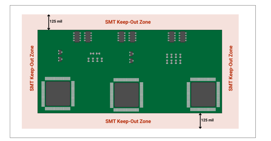

Standard component to edge spacing
Incorrect pad sizes and spacings
Buying a compact pad size could cause poor solder joints in SMT components.
The solution to this problem is not to make the pad as large as is feasible. A larger pad will make SMT parts move from all their position while soldering.
Thesleeping pad spacing can not be very close or far as it poses a problem while getting the components.
PCBA Silkscreen Errors
The silkscreen layer will be a major source info. Some cases include component orientation marks, polarity marks and cathode marks.
If details are missing or uncertain, then assembly houses will need to wait for a accurate data to become confirmed.
When the silkscreen has misprinted info like polarization plus the grouper installs parts accordingly, then a board might malfunction.
The legibility of the silkscreen must be good before assembly.

PCBA silkscreen printing specifications
PCBA High temperature errors
The warmth produced through the soldering process can break the table.
Thecontrol of the warmth produced is essential. Thermal cushioning for efficient heat dissipation.
PCBA DfM and DFA guidelines assist you to predict the style problems before the manufacturing process.
They might bewill definitely minimize the repercussions of fashion faults if they could be not completely foolproof.
If you desire to build a brand new PCBA, never miss the manufacturing and assembly steps.
FS Technologies’ online DFM inspection tool can be used to investigate board layouts.
Following these types of guidelines will help you help to make sure that you have a good manufacturable PCBA design.